I’ve been starting off in FPGA programming which is interesting, and honestly, I’d love to have some MakeICT people join me, because it’s interesting. I’m starting off on making an CPU core (Probably a partial AVR, because I’m kinda curious how it could do a few things it does.) in Verilog, from pretty much the ground up and I’ll see about documenting it and surrounding information here. Before people can follow along though they need some background, so here’s Part/Lesson 1, that’s kinda electronics, kinda math, and logic.
Don’t let that scare you though. FPGAs seem a great tool, that can do some things that microcontrollers can’t, and even CPUs have trouble with. They excel in cases of parallel operations, and low latency. Which is why I’m posting about it, and hopefully from a level which will let everyone follow along. I’m planning to post things like this weekly-ish, since I’m unlikely to be in the space until Covid is resolved.
If anyone wants to join how I’m doing the hardware, I’m using a repurposed board using a Zynq 7010, The board I am using is <$20 because it’s repurposed/used. It requires space for the (closed source) Vivado software (30GB needed for install +) and a 12V power supply. Email/Message me for link. (Not selling/making any money, but also don’t want to paste it all over and have the supply dry up, until friends who want one and now MakeICT people can get one.) Open Source Software is not quite there for the chip, thus Vivado. Almost. Alternatively, there are things like most anything under this: https://www.sparkfun.com/categories/136 and tons more options. (The prices are why I was so happy to find the boards I did!)
Little I plan on should be super specific to what I’m using. I’ll probably show how to configure the board, and I may demonstrate something using the Linux side, if I end up making a display for it. I’ve done whole software side of graphics from mostly scratch thing before and that wheel is one I don’t want to reinvent again, when there’s an easy way. (Telling Linux: This part of memory is a framebuffer, and GO!)
Binary Logic: Really Short Version
Theory
Now, Rather than go off on the electronics origin of binary logic, we are just going to, just accept that there are two voltage levels, which correspond to logic levels on any given wire. HIGH/LOW and 1/0. We will also gloss over transistors and how they work, because you can get into details, which are important for electronics working, but irrelevant at that moment. We are going to live in logic land, with fantasy physics.
For logic gates that are usable in computers, with two inputs/one output, We have essentially OR, XOR, AND, NAND, NOR, NXOR. (Some easier to do in chips than others, due to the aforementioned transistors but we’ll ignore that.) Let’s look at the most common ones of those: OR and AND first.
If you’ve got two inputs, A and B, which can be 1 or 0. For an AND gate, If both are 1, the logical output if both are 1, if not 0. For an OR gate, if one or both are 1, the logical output is 1, if not 0.
The above is kinda clunky. Fortunately, there’s a thing called a truth table (or logic table).
We can express ALL our inputs:
A | B
0 | 0
0 | 1
1 | 0
1 | 1
Then we can add our outputs:
A | B || OR | AND
0 | 0 ||  0 |   0
0 | 1 ||  1 |   0
1 | 0 ||  1 |   0
1 | 1 ||  1 |   1
Which is easier to tell.
Now the other logic functions: XOR is Exclusive OR so only 1 of the inputs is 1.
A | B || OR | AND | XOR
0 | 0 ||  0 |   0 |   0
0 | 1 ||  1 |   0 |   1
1 | 0 ||  1 |   0 |   1
1 | 1 ||  1 |   1 |   0
The N (Not) versions are not, reversed. So NAND (Not-AND) is 1 any time AND would be 0 and 0 anytime AND would be 1, similarly for NOR (Not-OR) and NXOR (Not-XOR)
A | B || OR | AND | XOR | NOR | NAND | NXOR*
0 | 0 ||  0 |   0 |   0 |   1 |    1 |    1
0 | 1 ||  1 |   0 |   1 |   0 |    1 |    0
1 | 0 ||  1 |   0 |   1 |   0 |    1 |    0
1 | 1 ||  1 |   1 |   0 |   0 |    0 |    1

* NXOR is sometimes XNOR, said as Exclusive NOR usually. It means the same thing, but as it fits in with Not-AND, Not-OR, Not-XOR. So however you want to say it. I'll use NXOR
So those are the logic functions that you get out of any of them. So useful?
Well, let’s do something simple, Binary Addition! Remembering that decimal=binary: 0=0, 1=1, 2=10, 3=11, 4=100, 5=101, 6=110, 7=111, 8=1000, etc.
A | B || ADD
0 | 0 ||   0
0 | 1 ||   1
1 | 0 ||   1
1 | 1 ||  10
Huh. We can’t represent that with 1 output. We need a second digit, so let’s separate them. Call it X, Y for now.
A | B || X | Y
0 | 0 || 0 | 0
0 | 1 || 0 | 1
1 | 0 || 0 | 1
1 | 1 || 1 | 0
So how do we make those outputs? Looking back at our Logic table added on:
A | B || X | Y || OR | AND | XOR | NOR | NAND | NXOR
0 | 0 || 0 | 0 ||  0 |   0 |   0 |   1 |    1 |    1
0 | 1 || 0 | 1 ||  1 |   0 |   1 |   0 |    1 |    0
1 | 0 || 0 | 1 ||  1 |   0 |   1 |   0 |    1 |    0
1 | 1 || 1 | 0 ||  1 |   1 |   0 |   0 |    0 |    1
X looks like AND, and Y looks like XOR
X = A AND B
Y = A XOR B
So yay, we’ve created something to add 2 1-bit numbers together. Let’s call it a half-adder. Woohoo! Wait? Half-Adder? Anyone guess why? I’ll go into it on the next post.
But let’s get back to LUTs, LUTs are Look Up Tables. Think kinda like using sin/cos look up tables, you may have used. You don’t calculate something simply output, you just
look it up. Look up tables are essentially flexible logic which let you go: For these inputs produce this output. They have in FPGAs between 3 and 6 inputs, and up to 2 outputs. For a 2 input LUT, You have 2^2 possible inputs, (needing 4 bits to configure it, per output), 3-input LUT 2^3, 4-input 2^4, etc. But the simple take away is we can do any of those logical functions per LUT. I’ll refer to them as nLUTi:o with i being input bits, o being output bits, with n being the # if referencing them. Note also that a 2 output LUT can generally act as two smaller ones.
LUTs are one of the cores of FPGAs, that make them so useful.
So if we feed A and B into 2 LUT2:1, we can configure them so that 1LUT = AND and 2LUT = XOR
A | B || 1LUT | 2LUT
0 | 0 ||    0 |    0
0 | 1 ||    0 |    1
1 | 0 ||    0 |    1
1 | 1 ||    1 |    0
So that’s how the FPGA will do it internally. Then there’s routing it to/from pins.
Another thing you can do is invert the input with a LUT1:1, if for some reason you need to. (This is something that’s more common in physical layouts, as with FPGAs, the next LUT it goes through, can deal with the inverted logic. For example in the above if A were inverted (!A) it could just use the !A column as inputs, as opposed to A.
A | !A | B || 1LUT | 2LUT
0 |  1 | 0 ||    0 |    0
0 |  1 | 1 ||    0 |    1
1 |  0 | 0 ||    0 |    1
1 |  0 | 1 ||    1 |    0
Now you generally don’t deal with things nearly that fine grained when writing for FPGAs. Since we aren’t using gates, but a look up table, it just changes what inputs produce what outputs. If we based it purely off gates, we’d need a NOT gate, aka an inverter. You could do a trick if you are using logic chips, which is a NAND gate with both inputs tied together acts as an inverter, we simply won’t need to. It is however, a great thing to remember for circuits.
But unless we want to go back to hand coding things, we’ll be relying on a language which uses logic. I’m going to use Verilog as it’s supported best by open source tools and commercial tools. There exists VHDL as well.
Practice
Let’s actually turn that theory into practice, even if it is simple!
So to create our 1-bit adder in what’s called a module. (You can think of it as a chip, that you don’t have to hook up to power/ground if you are familiar with logic chips.) We will ignore clocks, and any enable bits, as well as things like wires/registers that are a thing in Verilog, and will need to be added later. (Verilog is one of the languages used to program FPGAs and to generate ‘hard’ chips, which get produced with traditional methods.)
module half_adder (
input A,
input B,
output X,
output Y
);
endmodule
So that will do nothing. We have to tell it to do something and in our case since we have our simple logic from above, we can add that in, but we need to know what symbols there are in verilog (Also, shared with other programming languages, because every group decides to make up it’s own symbols, and worse for shorthand.)
AND &
OR |
XOR ^
NOT is a prefix of ~ around the results, but can be use with ~^
So if you have A, B, NAND would be ~(A & B), NOR would be ~(A | B), NXOR would be ~(A ^ B), but also could be A ~^ B, just because.
It can’t be directly used except in the case of NXOR
X = A AND B
Y = A XOR B
Become ( A double slash (//) indicates anything that follows on that line is a comment, something which you can read to understand, but will not affect the compiler. Also, lines end in semi-colons because it derives that from the C Programming Language)
X = A & B; // A AND B
Y = A ^ B; // A XOR B
Verilog allows us to use ‘assign’ to set a value here, so our full module becomes:
module half_adder (
input A,
input B,
output X,
output Y
);

    assign X = A & B; // A AND B
    assign Y = A ^ B; // A XOR B

endmodule
Yay, our first Verilog module! If we synthesized this and made it with two switches, and two leds, any time both were pushed you’d see one led (X) on, if one were pushed the other led (Y) on, and none on if nothing was pushed down.
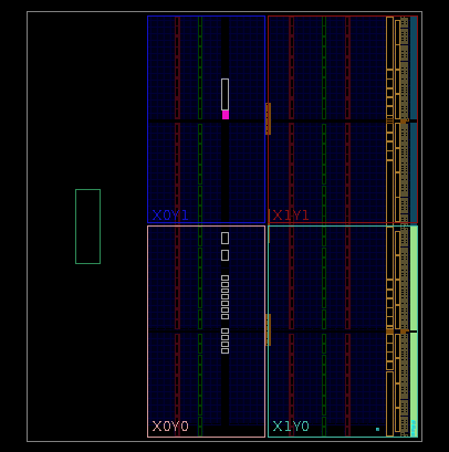
If it’s compiled into a design excluding the IO, The logic is all in the small blue dot in the lower right of X1Y0, of the chip I’m using (Xilinx Zynq 7010, has ~28k LUT6:2s and this all fits into a single LUT6:2 (operating as 2 LUT2:1s)). Screenshots using Vivado.
and here’s the schematic (IBUF/OBUF are the handling of IO pins):
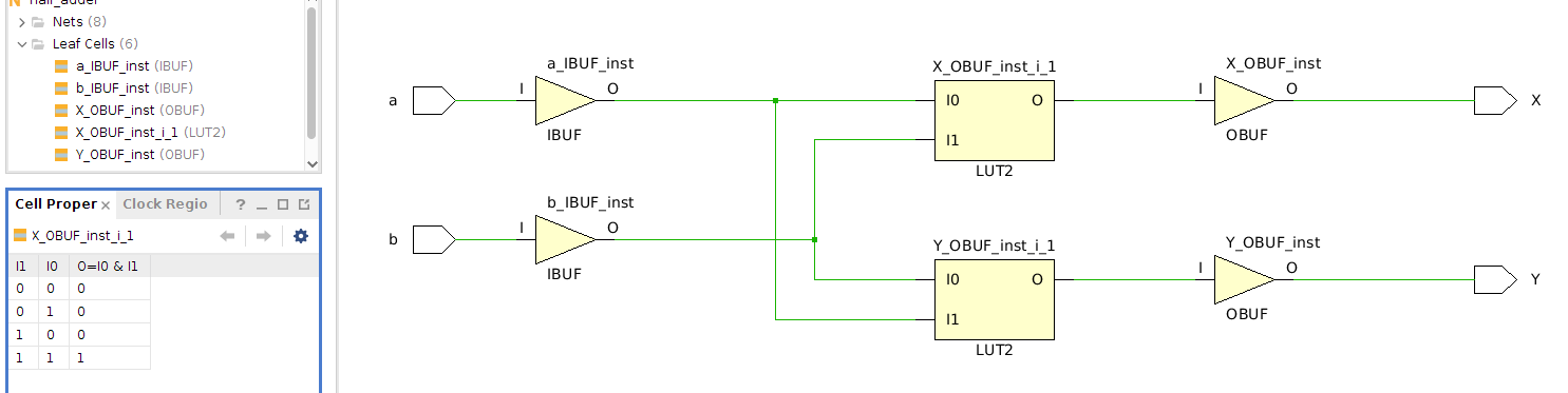
In the left, you can see the truth table for X, Here’s Y’s
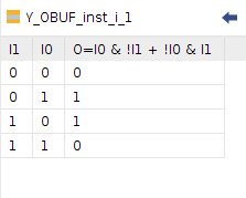
Hey! That looks kinda familiar! From above:
A | B || X | Y
0 | 0 || 0 | 0
0 | 1 || 0 | 1
1 | 0 || 0 | 1
1 | 1 || 1 | 0
I hadn’t found where the truth tables were in the software previously prior to the screen shots, but I figured they had to be somewhere, so went looking. It does give an equation, which is for X, Inputs: I0 & I1, but for Y it shows a bit differently: O=I0 & !I1 + !I0 & I1 (& = AND, ! = NOT, same as ~, and + in this case means OR) So, it breaks down as (A AND NOT B) OR (NOT A AND B) which logically works as XOR, but given that the same dialog showing the symbols also has an XOR… Really?
Cool Related Things
Some links to geek out on with regard to FPGA and CPU design, and generally cool things in their own right:
- https://www.youtube.com/channel/UCS0N5baNlQWJCUrhCEo8WlA - Ken Easter’s Youtube channel which goes over making computers on breadboards, and with a 6502 (really early chip) His videos are perhaps the clearest explanation I’ve seen in video form of a way to do CPUs, ever. (Though they are rather restricted (for reasons of simplicity.) It’s a major inspiration for this. You should probably check it out.
- https://www.righto.com/2020/09/reverse-engineering-first-fpga-chip.html - Breakdown of the first FPGA the Xilinx XC2064, which now would be pretty much considered a CLPD.
- https://zipcpu.com/ - Covers some aspects FPGA design of processors - https://zipcpu.com/blog/2017/08/21/rules-for-newbies.html - Though for compatibility, I’m probably going to need to break one of these.
- https://symbiflow.github.io/ - Symbiflow is the combination overall combination of several open source projects into one, listed below, How it works is described in
- http://www.clifford.at/yosys/ - Yosys To put it as simply as possible: The Verilog compiler.
- http://www.clifford.at/icestorm/ - Project Icestorm which supports the fairly small iCE40 devices
- https://github.com/SymbiFlow/prjtrellis - Project Trellis for the Lattice ECP5 chips
- https://github.com/SymbiFlow/prjxray - Project X-Ray is for the Xilinx series 7 chips to document them. Right now Symbiflow supports some of the Xilinx chips, due to the programming information not quite known yet.
Questions
Hopefully everyone followed that, who wanted to. Also that it wasn’t too overwhelming. If there’s anything unclear, questions, comments on my wiring job, too much/too little detail, or if you are simply interested in following this, comment and let me know. Apologies if this is jumbled, because of the editor making it hard to edit. (May throw this on the wiki, in the future). One internet point, If you can tell me why it’s a half-adder with or without looking it up.
